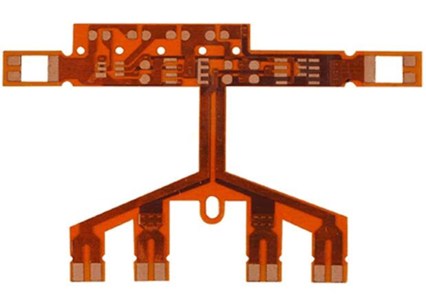
With the continuous updating of electronic products, fpc is more and more popular with most engineers, and the surface technology of fpc is more and more diverse. So what are the common surface treatments, and what are their advantages and disadvantages? Let's talk about them in detail.
1. Hot air leveling
This is a common and cheap treatment process. It refers to coating molten tin-lead solder on the surface of the circuit board and leveling (blowing) it with heating shrinkage air to make it a coating layer that can not only resist copper oxidation but also provide excellent solderability. Hot air leveling daily solder and copper at the fusion point will cause copper-tin metal compound.
Advantages: long storage time; After the completion of PCB, the copper surface is completely wetted (tin is completely covered before welding); Suitable lead-free welding; Mature process, low cost, suitable visual inspection and electrical measurement
Disadvantages: inappropriate line binding; Due to the surface flatness, there are limits on SMT; Unsuitable contact switch design. Copper will dissolve when tin is sprayed, and the board will withstand a high temperature. The unique thick or thin plate is limited by tin spraying, which is not easy to make and operate.
2. Organic Solderability Protector (OSP)
The general process is: degreasing -->micro-etching -->acid washing -->pure water washing -->organic coating -->washing, and the process control is relatively simple compared with the rest.
Advantages: simple manufacturing process, fairly flat surface, suitable for lead-free welding and SMT. Easy to rework, easy to make and operate, suitable for horizontal line operation. The board is suitable for coexistence of multiple processes (such as OSP ENIG). Low cost and friendly environment. Belonging to Qinji Group, Baineng is China's leading electronic household service platform. It provides a complete set of processing plans for electronic household supply chain, such as components, sensor acquisition, PCB customization, BOM allocation, material selection, etc. online, to meet the overall needs of small and medium-sized customers of electronic household products in a one-stop manner.
Disadvantages: The number of reflow soldering is limited (the film will be damaged if the thickness of reflow soldering is repeated, basically no problem for two times). Improper crimping technique, wire binding. Visual inspection and electrical measurement are not easy. N2 gas protection is required during SMT. SMT rework is not appropriate. High storage conditions are required.
3. Sinking silver
Advantages: simple manufacturing process, suitable for lead-free welding, SMT. The surface is quite flat, the cost is low, and the line is suitable and meticulous.
Disadvantages: high storage conditions and simple pollution. The welding strength is easy to have problems (micro void problem). The phenomenon of electromigration and the phenomenon of Jafani bite on the copper under the solder mask are easy to occur. Electrical measurement is also a problem.
4. Full plate nickel-plated gold
Advantage: longer storage time>12 months. Suitable contact switch design and gold wire binding. Proper electrical test
Defect: high capital, thick gold contrast. When electroplating gold fingers, special design lines are required to conduct electricity. Because the thickness of gold is not consistent, when it is used in welding, it may cause embrittlement of the solder joint and affect the strength. The average of the electroplating surface. The electroplated nickel gold does not cover the edge of the wire. Unsuitable aluminum wire binding.
5. Sink gold
The general process is: deacidification cleaning -->micro-etching -->pre-leaching -->activation -->electroless nickel plating -->electroless gold leaching; There are 6 chemical tanks in the process, which touch nearly 100 kinds of chemicals, and the process control is complex.
Advantages: It is not easy to oxidize, can be stored in light for a long time, and has a flat surface. It is suitable for welding fine-gap pins and components with small solder joints. The preferred PCB with buttons (such as mobile phone board). Repeated reflow soldering is not likely to reduce its solderability. It can be used as the base material for COB (Chip On Board) wiring.
Disadvantages: the cost is high and the welding strength is poor. Because of the use of electroless nickel plating process, it is easy to have a black disk problem. The nickel layer will oxidize with time, and the long-term reliability is a problem.
6. Sink tin
Advantages: suitable for horizontal line production. It is suitable for careful circuit processing, lead-free welding and unique crimping technology. Very good flatness, suitable for SMT.
Disadvantages: The storage conditions with good demand should not be more than 6 months to control the growth of tin whiskers. Unsuitable contact switch design. In terms of manufacturing process, the requirements for welding resistance film process are relatively high, otherwise the welding resistance film will be scattered. In case of repeated welding, N2 gas protection shall be compared. Electrical measurement is also a problem.

Online
Service
ConsultationTime:9:00-18:00
Hot
Line
0755-27847787
7*24H Service
Follow
Us
 Website