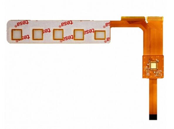
Mark point, also known as reference point, provides a common locatable circuit pattern for all steps in the FPC soft board assembly process. Therefore, the Mark point is crucial to SMT production. All SMT patch boards must have Mark points. So what should we pay attention to when designing? Let's talk about it in detail.
1. The shape requires Mark points to be marked as solid circles; A complete Mark point includes mark points (or characteristic points) and open areas. The minimum diameter of the mark size is 1.0mm, and the maximum diameter is 3.0mm. The size change of Mark point mark on the same printed board cannot exceed 25um.
2. Mark points are located at the diagonal relative position on the circuit board or combination board and separated as far as possible. It is best to be distributed at the longest diagonal position; In order to meet the requirements of SMT mounting accuracy, the FPC flexible circuit board must have at least one pair of mark points that meet the design requirements and can be recognized by SMT machines, that is, there must be a single mark.
3. The distance between the mark point (edge) and the edge of the printed board must be ≥ 5.0mm (the minimum spacing requirement for machine clamping FPC), and must be in the FPC board rather than at the board edge, and meet the minimum mark point clearance requirement. Emphasis: the distance between the edge of the Mark point and the edge of the plate is ≥ 5.0mm, not the center of the Mark point.
4. There must be an open area without other circuit features or marks around the Mark point mark. The radius of the open area circle r ≥ 2R, R is the radius of the Mark point. When r reaches 3R, the machine recognition effect is better. It is often found that the open area of the Mark point is blocked by the character layer or cut by the V-CUT, which makes the SMT machine unable to recognize.
5. Mark point marks can be bare copper, bare copper protected by clear anti-oxidation coating, nickel or tin plating, or solder coating. The surface flatness of the Mark point mark should be within 15um. The best performance can be achieved when there is a high contrast between the Mark point mark and the substrate material of the printed board. The inner background of all Mark points must be the same.

Online
Service
ConsultationTime:9:00-18:00
Hot
Line
0755-27847787
7*24H Service
Follow
Us
 Website